Complete wet etching system for porous silicon formation
Porous silicon (PS) has gained wide-spread attention over the last decade for its interesting material properties, including nanometer features and extremely high specific surface area. Applications are, amongst others, humidity sensors, particle filters, optical elements and biochemical matrices. Microporous silicon is fabricated by etching silicon in HF-based solutions under applied voltage. Most fabrication processes for macroporous silicon need illumination in addition, an issue also addressed by AMMTs tools for PS formation.
AMMT’s line of PS equipment consists of:
Together, these products form a turn-key system for porous silicon etching, which is used by major players in the MEMS field.
For details please see the product pages.
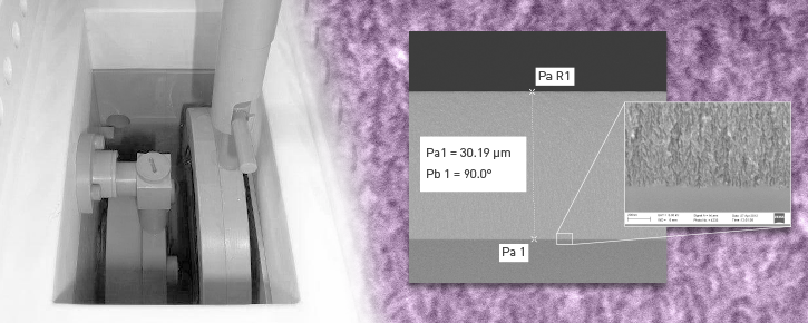
Click to enlarge
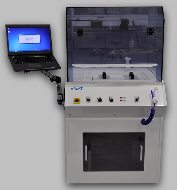
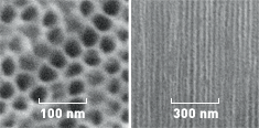
Figure_ n+ -type porous silicon made by anodization at 250 mA/cmin the dark in an ethanoic/HF bath: (left) SEM porous silicon front view; (right) SEM porous silicon cross-section view.
